2.4 Illustration of piezoelectricity in statics: patch example
2.4.1 Patch in extensional mode
Consider a thin piezoelectric patch of dimensions b x h x w. The poling direction, noted 3 in the IEEE Standards on piezoelectricity is perpendicular to the plane of the piezoelectric patch. Continuous electrodes are present on the top and bottom surfaces (z=0, z=h) so that the electric potential is constant on these surfaces and denoted by V1 and V2 respectively. We assume that a difference of potential is applied between the electrodes, resulting in an electric field parallel to the poling direction and equal to (Figure 2.5)
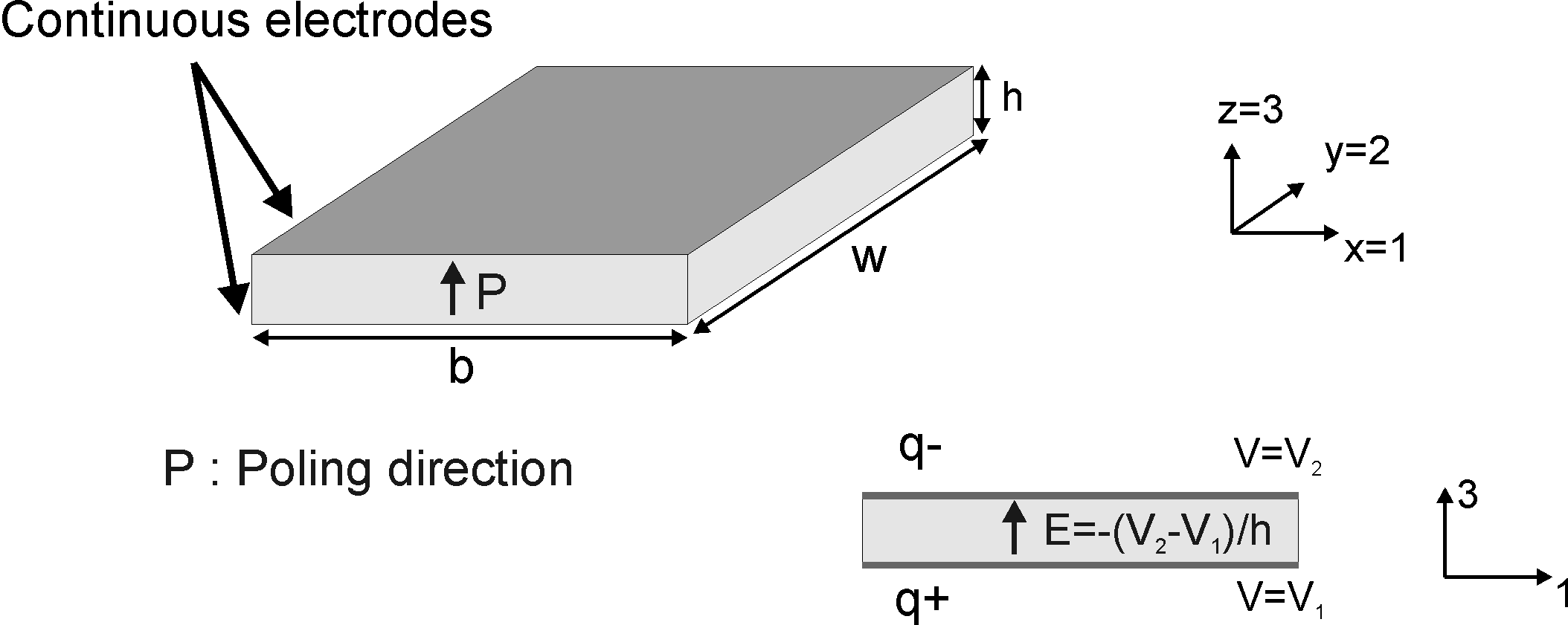
| Figure 2.5: A piezoelectric patch poled through the thickness with continuous electrodes on the top and bottom surfaces |
We adopt the following expression for the constitutive equations:
The patch is assumed to be unconstrained so that it can expand freely, leading to {T}=0, so that we have :
We have taken into account the fact that the electric field is in the z-direction only. This shows that when applying a difference of potential across the thickness (in the poling direction), strains will be induced in the directions 1,2, and 3. The magnitude of these different strains is proportional to the d3i coefficients of the piezoelectric material. For a ceramic PZT material, d31=d32<0, and d33>0 and is generally between 2 and 3 times larger in magnitude than d31 and d32.
The second equation can be used in order to assess the amount of charge that is accumulated on both electrodes. We have :
The only non-zero component of the D vector is D3 given by :
The charge accumulated on the electrode is given by :
where {n} is the normal to the electrode. For the top electrode, this leads to :
where A is the surface of the electrode. For the bottom electrode
When (V1−V2) is positive, the electric field is in the direction of poling and the charge on the top electrode is negative, while the charge accumulated on the bottom electrode is positive (Figure 2.5). Note that this equation corresponds to the equation linking the charge to the difference of potential for a capacitor (q=C Δ V). The value of the capacitance is therefore :
which corresponds to the capacitance of the free piezoelectric patch ({T}=0).
If we now consider the case where the piezoelectric patch is fully mechanically constrained ({S}=0
), we have:
leading to :
The fact that the patch is not allowed to expand is responsible for the generation of internal stresses which are proportionnal to the e3i coefficients.
In this case, the capacitance is given by:
which corresponds to the capacitance of the constrained piezoelectric patch ({S}=0). This illustrates the fact that the capacitance of a piezoelectric patch depends on the mechanical boundary conditions. This is not the case for other types of dielectric materials in which the piezoelectric effect is not present, and for which therefore the capacitance is independent on the mechanical strain or stress.
2.4.2 Patch in shear mode
We now consider the same patch but where the polarization is in the plane of the actuator, as represented in Figure 2.6.
As in the previous example, continuous electrodes are present on the top and bottom surfaces (z=0, z=h) so that the electric potential is constant on these surfaces and denoted by V1 and V2 respectively. We assume that a difference of potential is applied between the electrodes, resulting in an electric field perpendicular to the poling direction and equal to
The electric field is now applied in direction 2, so that it will activate the shear d24=d15 mode of the piezoelectric material.
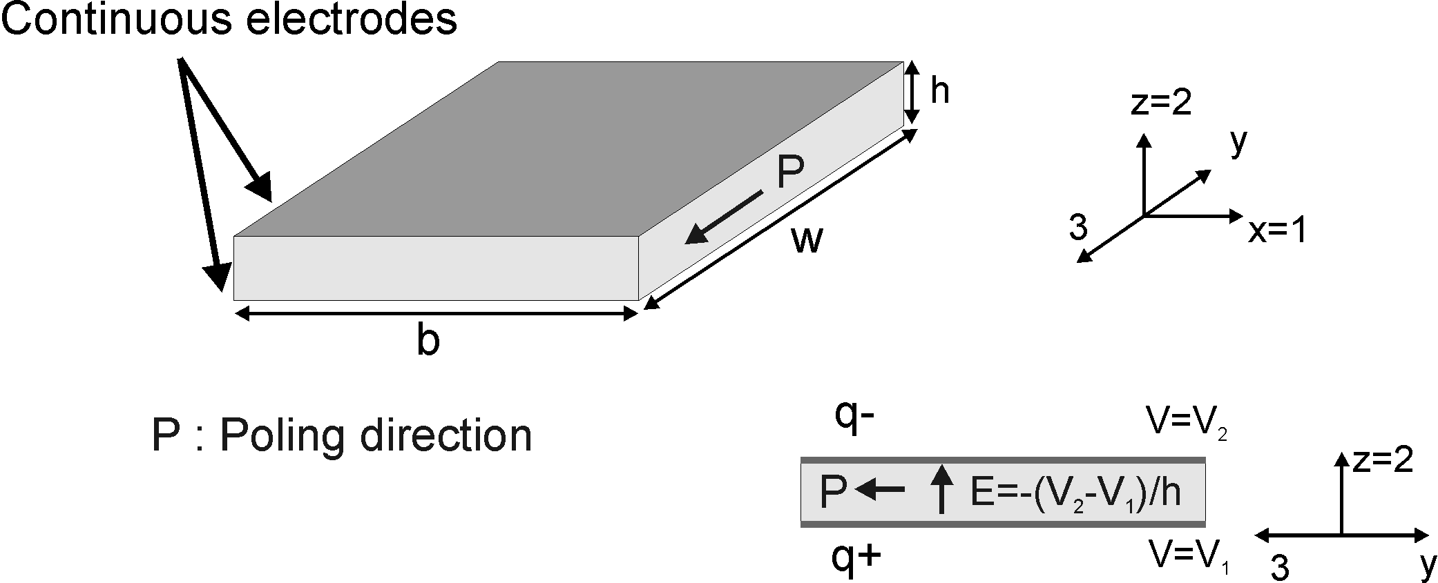
| Figure 2.6: A piezoelectric patch poled in the plane with continuous electrodes on the top and bottom surfaces |
The patch is assumed to be unconstrained so that it can expand freely, leading to {T}=0, so that we have :
We have taken into account the fact that the electric field is in the z-direction only, corresponding to direction 2 in the local axis of the piezoelectric material (direction 3 is the poling direction by convention). This shows that when the patch is poled in the plane, when applying a difference of potential across the thickness, a shear strain in the local 23 plane will be induced. The magnitude of this strain is proportional to the d24 coefficient of the piezoelectric material.
The second equation can be used in order to assess the amount of charge that is accumulated on both electrodes. We have :
The only non-zero component of the D vector is D2 given by :
The charge accumulated on the electrode is given by :
where {n} is the normal to the electrode. For the top electrode, this leads to :
where A is the surface of the electrode. For the bottom electrode
When (V1−V2) is positive, the charge on the top electrode is negative, while the charge accumulated on the bottom electrode is positive (Figure 2.6). The value of the capacitance is therefore:
which corresponds to the capacitance of the free piezoelectric patch ({T}=0) and is close to the capacitance when the poling is out of the plane of the transducer because є22T≃є33T (in reality, there is typically a difference of 5% between these two values so that the capacitance will be slightly different).
If we now consider the case where the piezoelectric patch is fully mechanically constrained ({S}=0
), we have:
leading to :
In this case, the capacitance is given by:
which corresponds to the capacitance of the constrained piezoelectric patch activated in shear ({S}=0). Note that this capacitance is clearly different from CS when the poling is out of the plane, because the value of є22S is very different from the value of є33S, due to the different values of stiffness and piezoelectric coefficients in shear and extensional mode.
©1991-2025 by SDTools


