1.2 Basics of piezoelectricity
Polarization consists in the separation of positive and negative electric charges at different ends of the dielectric material on the application of an external electric field (Figure 1.1).
Spontaneous polarization is the phenomenon by which polarization appears without the application of an external electric field. Spontaneous polarization has been observed in certain crystals in which the centers of positive and negative charges do not coincide. Spontaneous polarization can occur more easily in perovskite crystal structures.
The level and direction of the polarization is described by the electric displacement vector D:
where P is the permanent polarization which is retained even in the absence of an external electric field, and є E represents the polarization induced by an applied electric field. є is the dielectric permittivity. If no spontaneous polarization exists in the material, the process through which permanent polarization is induced in a material is known as poling.

| Figure 1.1: Polarization: separation of positive and negative electric charges on the two sides of a dielectric material |
Ferroelectric materials have permanent polarization that can be altered by the application of an external electric field, which corresponds to poling of the material. As an example, perovskite structures are ferroelectric below the Curie temperature. In the ferroelectric phase, polarization can therefore be induced by the application of a (large) electric field.
Piezoelectricity was discovered by Pierre and Jacques Curie in 1880. The direct piezoelectric effect is the property of a material to display electric charge on its surface under the application of an external mechanical stress (i.e. to change its polarization). (Figure 1.2a).
The converse piezoelectric effect is the production of a mechanical strain due to a change in polarization (Figure 1.2b).
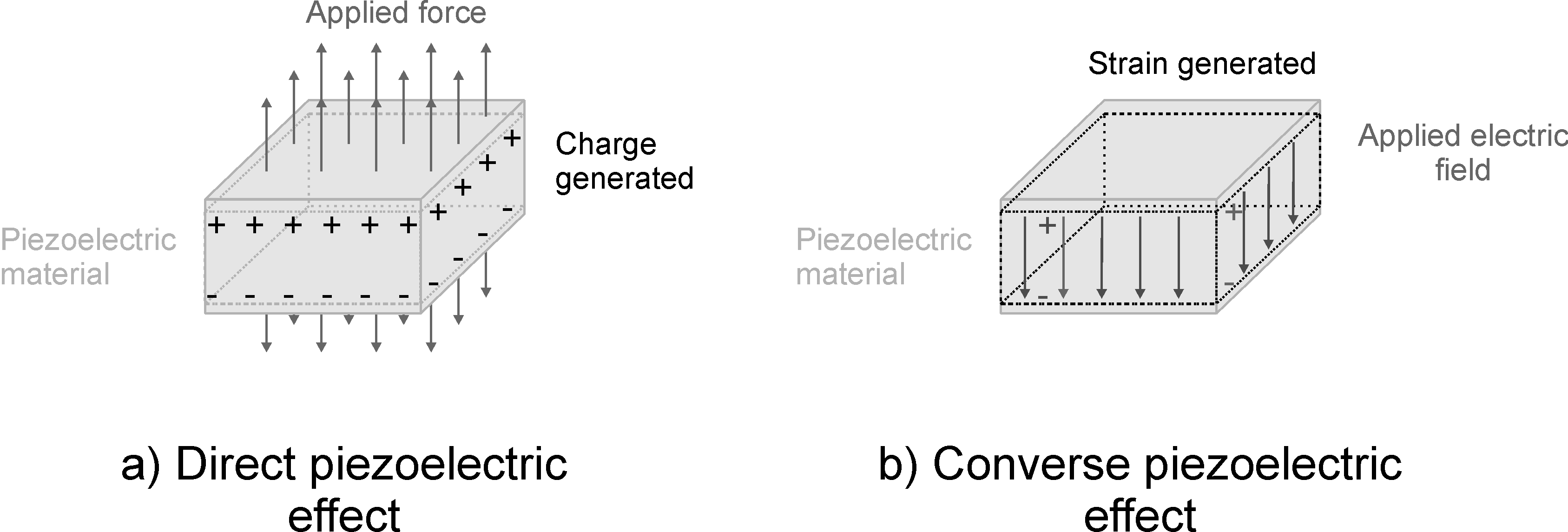
| Figure 1.2: Direct and converse piezoelectric effect |
Piezoelectricity occurs naturally in non ferroelectric single crystals such as quartz, but the effect is not very strong, although it is very stable.
The direct effect is due to a distortion of the crystal lattice caused by the applied mechanical stress resulting in the appearance of electrical dipoles. Conversely, an electric field applied to the crystal causes a distortion of the lattice resulting in an induced mechanical strain. In other materials, piezoelectricity can be induced through poling. This can be achieved in ferroelectric crystals, ceramics or polymers.
A piezoelectric ceramic is produced by pressing ferroelectric material grains (typically a few micrometers in diameter) together. During fabrication, the ceramic powder is heated (sintering process) above Curie temperature. As it cools down, the perovskite ceramic undergoes phase transformation from the paraelectric state to the ferroelectric state, resulting in the formation of randomly oriented ferroelectric domains . These domains are arranged in grains, containing either 90° or 180° domains (Figure 1.3a). This random orientation leads to zero (or negligible) net polarization and piezoelectric coefficients (Figure 1.3b)).
a) b)

| Figure 1.3: Piezoelectric ceramic : a) ferroelectric grains and domains, b) distribution of poling directions |
The application of a sufficiently high electric field to the ceramic causes the domains to reorient in the direction of the applied electric field. Note however that the mobility of the domains is not such that all domains are perfectly aligned in the poling direction, but the total net polarization increases with the magnitude of the electric field (Figure 1.4). After removal of the applied electric field, the ferroelectric domains do not return in their initial orientation and a permanent polarization remains in the direction of the applied electric field (the poling direction). In this state, the application of a moderate electric field results in domain motions which are responsible for a deformation of the ceramic and are the source of the piezoelectric effect.
The poling direction is therefore a very important material property of piezoelectric materials and needs to be known for a proper modeling.

| Figure 1.4: Orientation of the ferroelectric domains in non-polarized and polarized ceramics |
Typical examples of simple perovskites are Barium titanate (BaTiO3) and lead titanate (PbTiO3). The most common perovskite alloy is lead zirconate titanate (PZT- PbZr TiO3). Nowadays, the most common ceramic used in piezoelectric structures for structural dynamics applications (active control, shape control, structural health monitoring) is PZT, which will be used extensively in the documented examples.
In certain polymers, piezoelectricity can be obtained by orienting the molecular dipoles within the polymer chain. Similarly to the ferroelectric domains in ceramics, in the natural state, the molecular dipole moments usually cancel each other resulting in an almost zero macroscopic dipole. Poling of the polymer is usually performed by stretching the polymer and applying a very high electric field, which causes the molecular dipoles to orient with the electric field, and remain orientated in this preferential direction after removal of the electric field (permanent polarization). This gives rise to piezoelectricity in the polymer. The technology of piezoelectric polymers has been largely dominated by ferroelectric polymers from the polyvinylidene fluoride (PVDF) family, discovered in 1969. The main advantage is the good flexibility, but their piezoelectric coefficients are much lower compared to ferroelectric ceramics.
1.2.1 Piezoelectric constitutive laws in 3D
Up to a certain level of electric field and strain, piezoelectric materials behave linearly. This tutorial is restricted to linear piezoelectricity, but the interested reader can refer to [1] for more details on non-linear piezoelectricity.
Assuming a linear piezoelectric material and adopting the notations of the IEEE Standards on piezoelectricity [2], the 3D constitutive equations are given by:
where Ei and Di are the components of the electric field
vector and the electric displacement vector, and Ti and Si
are the components of stress and strain vectors, defined according
to:
Matrix notations are usually adopted leading to:
A widely used alternative and equivalent representation consists in writing the constitutive equations in the following form:
where the following relationships hold:
There are also two additional possibilities to write these constitutive equations, which are less commonly used but are given here for completeness:
The following relationships hold:
The piezoelectric coefficients are contained in the matrix [d] whose structure is specific to each type of piezoelectric material. The typical structure for a z-polarized PZT material is
Regular PZT ceramics are isotropic in the plane perpendicular to the poling direction (d31=d32, d15=d24), but piezoelectric composites can have orthotropic properties [3].
PVDF material does not exhibit piezoelectricity in the shear mode, so that the typical structure is:
PVDF can be either isotropic or orthotropic in the plane perpendicular to the poling direction, depending on the fabrication process (uni-axial or bi-axial). Table 1.1 gives typical piezoelectric coefficients for PZT ceramics and PVDF films. Note that these properties can vary significantly from the figures in the table, as there are many different material types. The permittivity is usually given with its relative value which is the ratio of the permittivity by the permittivity of vacuum (є0=8.854 10−12 F/m).
| Material properties | PZT | PVDF (bi-axial) |
| Piezoelectric properties |
| d33 (pC/N) | 440 | -25 |
| d31 (pC/N) | -185 | 3 |
| d32 (pC/N) | -185 | 3 |
| Relative permittivity |
| єr | 1800 | 12 |
| Young's Modulus |
| Y1(GPa) | 54 | 3 |
| Y2(GPA) | 54 | 3 |
| Y3(GPA) | 48 | 10 |
| ρ (kg/m3) | 7600 | 1800 |
| Table 1.1: Typical piezoelectric properties of PZT ceramics and PVDF films |
1.2.2 Piezoelectric constitutive laws in plates
When thin piezoelectric transducers are used with plate structures, the common plane stress hypothesis (T3=0) must be used together with an hypothesis for the electric field. When the ceramic is poled through the thickness, the hypothesis commonly adopted is that the electric field is zero in the plane of the transducer (E1=E2=0). The constitutive equations then reduce to:
where the superscript * denotes the properties under the "piezoelectric plates" hypothesis (T3=E1=E2=0). These properties are related to the 3D properties with the following relationships:
The distinction is very important, as it is often not well understood and many errors can arise from the confusion between plate and 3D properties
of piezoelectric materials. Note however that the dij, sijE and єT coefficients are equal for plate and 3D constitutive equations. It is therefore preferable to handle the material properties of piezoelectric materials in the form of (5).
Similarly to the 3D equations, the constitutive equations can be written in a matrix form, separating the mechanical and the electrical parts:
|
| | {T} = | ⎡
⎣ | cE* | ⎤
⎦ | {S} − | ⎡
⎣ | e* | ⎤
⎦ | T{E}
|
| | | |
| {D} = | ⎡
⎣ | e* | ⎤
⎦ | {S} + | ⎡
⎣ | єS* | ⎤
⎦ | {E}
|
| | | (23) |
|
Using (7) in equations ((20),(21),(22)), one can further show that
and for the permittivity:
with
and
The values of e31*, e32* and є33S* can therefore be computed knowing the elastic matrix [cE* ]
and the values of d31 and d32 and є33T
1.2.3 Database of piezoelectric materials
m_piezo Dbval includes a number of material characteristics for piezoelectric materials. The properties are obtained from the datasheet of the material, but as we will illustrate, the data is not always sufficient to calculate all the material properties needed for the computations. Most of the information in the datasheet is generally related to the constitutive equations written in the form of (5).
For PZT, PVDF, or piezoelectric composites based on PZT and PVDF, the general form of these matrices is:
For an orthotropic material, the compliance matrix [sE] can be written as a function of the engineering constant Ei,νij and Gij as follows:
where z is aligned with the poling direction 3, and x,y with directions 1,2 respectively. Note that the matrix is symmetric so that:
A bulk piezoelectric ceramic exhibits transverse isotropic properties: the properties of the material are the same in the plane perpendicular to the poling direction. In this case, the compliance matrix reduces to:
and due to the symmetry we have:
where the subscript p refers to the in-plane properties. The matrix of piezoelectric coefficients is:
and the matrix of dielectric permittivities:
In order to use such a piezoelectric material in a 3D model, it is therefore necessary to have access to the 5 elastic constants Ep,Ez,νp,νzp and Gzp, 3 piezoelectric constants d31,d33, and d15 and two dielectric constants є11T,є33T. Unfortunately, such constants are generally not given in that form, but can be calculated from the material properties found in the datasheet.
It is important to introduce the electromechanical coupling factors which are generally given in the datasheet and are a function of the elastic, piezoelectric and dielectric properties of the material. They measure the effectiveness of the conversion of mechanical energy into electrical energy (and vice-versa). There is one coupling factor for each piezoelectric mode:
In addition, coupling factors kp for radial modes of thin discs, and kt for thickness modes of arbitrary shaped thin plates are also commonly given in datasheet. kp is related to k31 through:
kt is always lower than k33 but there does not seem to be a simple explicit expression of kt as a function of the material properties. The fact that kt is lower than k33 means that electrical energy conversion in the d33-mode is less effective for a thin plate than for a rod.
The definition of the coupling factors k33 and k15 also allows to write alternative expressions:
We illustrate the use of these different relationships to form the full set of mechanical, piezoelectric and dielectric properties for the material SONOX P502 from Ceramtec . The properties found in the datasheet are given in Table 1.2 (http://www.ceramtec.com/).
| Material property | value | unit |
| Piezoelectric properties |
| d33 | 440 | 10−12 m/V |
| d31 | -185 | 10−12 m/V |
| d15 | 560 | 10−12 m/V |
| e33 | 16.7 | C/m2=As/m2 |
| g33 | 26.9 10−3 | Vm/N |
| Permittivity |
| є33T | 1850 є0 | F/m |
| є33S | 875 є0 | F/m |
| є11T | 1950 є0 | F/m |
| є11S | 1260 є0 | F/m |
| Elastic properties |
| s11E | 18.5 10−12 | m2/N |
| s33E | 20.7 10−12 | m2/N |
| c33D | 15.7 1010 | N/m2 |
| c55D | 6.5 1010 | N/m2 |
| Coupling coefficients |
| k33 | 0.72 | |
| k15 | 0.74 | |
| k31 | 0.33 | |
| kp | 0.62 | |
| kt | 0.48 | |
| Density |
| ρ | 7740 | kg/m3 |
| Table 1.2: Properties of SONOX P502 from the datasheet |
Ep and Ez are computed directly from the definitions of s11E and s33E:
Knowing the value of s11E, d31, є33T and kp, s12E can be computed:
allowing to compute the value of νp:
and the value of Gp
From the value c55D and k15, we compute
from which the the value of Gzp is computed:
The value of νzp cannot be calculated from the datasheet information. We therefore assume that, as for most PZT ceramics:
The value of νpz is calculated as:
The complete set of values is summarized in Table 1.3. These are the values used in m_piezo. Note that there is some redundancy in the data from the datasheet, which allows to check for consistency. The two following coupling factors are computed from the data available and checked against the tabulated values.
The values are close to the values in Table 1.2. In addition, the value of g33 is given by:
and corresponds exactly to the value tabulated.
The value of e33 can be computed using Equation (7), leading to:
where there is a difference of about 15% with the tabulated value of e33= 16.7 C/m2.
Using (37) to compute k15 with the values from the datasheet, one gets:
which shows the non-consistency of the value of є11S in the datasheet. In fact, when computed using (8), one gets:
| Material property | value | unit |
| Piezoelectric properties |
| d33 | 440 | 10−12 m/V |
| d31 | -185 | 10−12 m/V |
| d15 | 560 | 10−12 m/V |
| Permittivity |
| є33T | 1850 є0 | F/m |
| є11T | 1950 є0 | F/m |
| Mechanical properties |
| Ep | 54.05 | GPa |
| Ez | 48.31 | GPa |
| Gzp | 29.41 | GPa |
| Gp | 19.17 | GPa |
| νp | 0.4124 | |
| νzp | 0.39 | |
| νpz | 0.44 | |
| ρ | 7740 | kg/m3 |
| Table 1.3: Properties of SONOX P502 to be used in 3D finite element models |
From the input values used in m_piezo, it is possible to compute the mechanical, piezoelectric and permittivity matrices used in the four different forms of the constitutive equations (4),(5),(9),(10) using the relationships (6)-(8)) and (11)-(13). The command p_piezo('TabDD') can be used in order to have access to all the matrices from the input values in m_piezo. This will be illustrated in section 1.2.5.
As the mechanical properties of PZT are not strongly orthotropic, a simplification can be done by considering that the material is isotropic (for the mechanical and dielectric properties, not the piezoelectric properties). An isotropic version of SONOX P502 is included in m_piezo under the name of SONOX_P502_iso whose properties are given in Table 1.4.
| Material property | value | unit |
| Piezoelectric properties |
| d33 | 440 | 10−12 m/V |
| d31 | -185 | 10−12 m/V |
| d15 | 560 | 10−12 m/V |
| Permittivity |
| єT | 1850 є0 | F/m |
| Mechanical properties |
| E | 54.05 | GPa |
| ν | 0.41 | |
| ρ | 7740 | kg/m3 |
| Table 1.4: Simplified material properties for SONOX P502 considering mechanical isotropy |
The second example is the PIC 255 PZT from PI ceramics. The properties found in the datasheet are given in Table 1.5 (http://www.piceramic.com/pdf/piezo_material.pdf). Note that C33D is not given in the datasheet, therefore we estimated it from the value of PIC 155 given in the same datasheet, which is just slightly stiffer.
| Material property | value | unit |
| Piezoelectric properties |
| d33 | 400 | 10−12 m/V |
| d31 | -180 | 10−12 m/V |
| d15 | 550 | 10−12 m/V |
| g31 | -11.3 10−3 | Vm/N |
| g33 | 25 10−3 | Vm/N |
| Permittivity |
| є33T | 1750 є0 | F/m |
| є11T | 1650 є0 | F/m |
| Elastic properties |
| s11E | 16.1 10−12 | m2/N |
| s33E | 20.7 10−12 | m2/N |
| c33D | 11 1010 | N/m2 |
| Coupling coefficients |
| k33 | 0.69 | |
| k15 | 0.66 | |
| k31 | 0.35 | |
| kp | 0.62 | |
| kt | 0.47 | |
| Density |
| ρ | 7800 | kg/m3 |
| Table 1.5: Properties of PIC 255 from the datasheet |
Ep and Ez are computed directly from the definitions of s11E and s33E:
Knowing the value of s11E, d31, є33T and kp, s12E can be computed:
allowing to compute the value of νp:
and the value of Gp
The value of s55E can be computed as:
which leads to:
Again, the value of νzp cannot be calculated from the datasheet information. We cannot assume a value of 0.39 as previously, as it would lead to a non-physical value of νpz. As νp is in the range of 0.32 and νzp is typically slightly lower, we assume that :
The value of νpz is calculated as:
The complete set of values is summarized in Table 1.6. These are the values used in m_piezo. Note that there is some redundancy in the data from the datasheet, which allows to check for consistency. The two following coupling factors are computed from the data available and checked against the tabulated values.
The values are very close to the values in Table 1.5. In addition, the value of g33 and g31 are given by:
and are also very close to the values tabulated.
| Material property | value | unit |
| Piezoelectric properties |
| d33 | 400 | 10−12 m/V |
| d31 | -180 | 10−12 m/V |
| d15 | 550 | 10−12 m/V |
| Permittivity |
| є33T | 1750 є0 | F/m |
| є11T | 1650 є0 | F/m |
| Mechanical properties |
| Ep | 62.11 | GPa |
| Ez | 48.31 | GPa |
| Gzp | 21.03 | GPa |
| Gp | 23.53 | GPa |
| νp | 0.3242 | |
| νzp | 0.30 | |
| νpz | 0.39 | |
| ρ | 7800 | kg/m3 |
| Table 1.6: Properties of PIC 255 to be used in 3D finite element models |
As shown in the derivations above, the datasheet for PZT material typically do not contain the full information to derive all the coefficients needed for computations, and some hypothesis need to be made. In addition, it is usual to have a variation of 10 % or more on these properties from batch to batch, and the datasheet are not updated for each batch. Note also that the properties are given at 20 °C and are temperature dependant. The variations with temperature are rarely given in the datasheet. This may also account for inaccuracies in the computations.
1.2.4 Illustration of piezoelectricity in statics: patch example
Consider a thin piezoelectric patch of dimensions b x h x w. The poling direction, noted 3 in the IEEE Standards on piezoelectricity is perpendicular to the plane of the piezoelectric patch. Continuous electrodes are present on the top and bottom surfaces (z=0, z=h) so that the electric potential is constant on these surfaces and denoted by V1 and V2 respectively. We assume that a difference of potential is applied between the electrodes, resulting in an electric field parallel to the poling direction and equal to

| Figure 1.5: A piezoelectric patch poled through the thickness with continuous electrodes on the top and bottom surfaces |
Assume that a constant difference of electric potential is applied to the two electrodes of the piezoelectric patch, as illustrated in Figure 1.5. We adopt the following expression for the constitutive equations:
The patch is assumed to be unconstrained so that it can expand freely, leading to {T}=0, so that we have :
We have taken into account the fact that the electric field is in the z-direction only. This shows that when applying a difference of potential across the thickness (in the poling direction), strains will be induced in the directions 1,2, and 3. The magnitude of these different strains is proportional to the d3i coefficients of the piezoelectric material. For a ceramic PZT material, d31=d32<0, and d33>0 and is generally between 2 and 3 times larger in magnitude than d31 and d32.
The second equation can be used in order to assess the amount of charge that is accumulated on both electrodes. We have :
The only non-zero component of the D vector is D3 given by :
The charge accumulated on the electrode is given by :
where {n} is the normal to the electrode. For the top electrode, this leads to :
where A is the surface of the electrode. For the bottom electrode
When (V1−V2) is positive, the electric field is in the direction of poling and the charge on the top electrode is negative, while the charge accumulated on the bottom electrode is positive (Figure 1.5). Note that this equation corresponds to the equation linking the charge to the difference of potential for a capacitor (q=C Δ V). The value of the capacitance is therefore :
which corresponds to the capacitance of the free piezoelectric patch ({T}=0).
If we now consider the case where the piezoelectric patch is fully mechanically constrained ({S}=0
), we have:
leading to :
In this case, the capacitance is given by:
which corresponds to the capacitance of the constrained piezoelectric patch ({S}=0). This illustrates the fact that the capacitance of a piezoelectric patch depends on the mechanical boundary conditions. This is not the case for other types of dielectric materials in which the piezoelectric effect is not present, and for which therefore the capacitance is independent on the mechanical strain or stress.
1.2.5 Numerical illustration : rectangular patch in statics
In this very simple example, the electric field and the strains are all constant, so that the electric potential and the displacement field are linear. It is therefore possible to obtain an exact solution using a single volumic 8-node finite element (with linear shape functions, the nodal unknowns being the displacements in x,y and z and the electric potential φ). Consider a piezoelectric patch whose dimensions and material properties are given in Table 1.7. The material properties correspond to the material SONOX_P502_iso in m_piezo.
| Property | Value |
| b | 10 mm |
| w | 10 mm |
| h | 2 mm |
| E | 54 GPa |
| ν | 0.44 |
| d31=d32 | -185 10−12 pC/N (or m/V) |
| d33 | 440 10−12 pC/N (or m/V) |
| d15=d24 | 560 10−12 pC/N (or m/V) |
| є33T=є22T=є11T | 1850 є0 |
| є0 | 8.854 10−12 Fm−1 |
| Table 1.7: Geometrical and material properties of the piezoelectric patch |
We first produce the mesh, associate the material properties and define the electrodes with  d_piezo('TutoPatch-s1')
. The default material is SONOX_P502_iso. The number of elements in the x, y and z directions are given by nx,ny and nz.
model=d_piezo('MeshPatch lx=1e-2 ly=1e-2 h=2e-3 nx=1 ny=1 nz=1');
model=p_piezo('ElectrodeMPC Top -ground',model,'z==2e-3');
model=p_piezo('ElectrodeMPC Bottom -Input "Free patch"',model,'z==0');
The information about the nodes associated to each electrode can be obtained through the following call:
p_piezo('TabInfo',model)
The material can be changed for example to PIC_255 with the following call, and the full set of mechanical, piezoelectric and permittivity matrices can be obtained in order to check consistency with the datasheet ( d_piezo('TutoPatch-s2')
):
model.pl=m_piezo('dbval 1 -elas 2 PIC_255');
p_piezo('TabDD',model)
The next step consists in defining the boundary conditions and load case using
 d_piezo('TutoPatch-s3')
. We consider here two cases, the first one where the patch is free to expand, and the second one where it is mechanically constrained (all mechanical degrees of freedom are equal to 0).
model=stack_set(model,'info','Freq',10);
def=fe_simul('dfrf',model); def.lab={'Free patch, axial'};
def.fun=[0 1]; def=feutil('rmfield',def,'data','LabFcn');
def=d_piezo('scriptFullConstrain',model,def);
def.lab{2}='Constrained patch, axial';
We can look at the deformed shape, and plot the electric field for both cases.
( d_piezo('TutoPatch-s4')
cf=feplot(model,def);
p_piezo('viewElec EltSel "matid1" DefLen 20e-4 reset',cf);
fecom('colormap',[1 0 0]);fecom('undef line');iimouse('resetview');

| Figure 1.6: Vizualisation of the electric field and deformed shape for the free patch under unit voltage excitation |
For the free patch deformed shape, we compute the mean strains from which d31, d32 and d33 are deduced. The values are found to be equal to the analytical values used in the model. Note that the parameters of the constitutive equations can be recovered using ( d_piezo('TutoPatch-s5')
):
CC=p_piezo('viewdd -struct',cf);
where the fields of CC are self-explanatory. The parameters which are not directly defined are computed from the equations presented in Section 1.2.1.
a=p_piezo('viewstrain -curve -mean',cf);
fprintf('Relation between mean strain on free structure and d_3i\n');
E3=a.Y(9,1); disp({'E3 mean' a.Y(9,1) 1/2e-3 'E3 analytic'})
disp([a.X{1}(1:3) num2cell([a.Y(1:3,1)/E3 CC.d(3,1:3)']) ...
{'d_31';'d_32';'d_33'}])
For the constrained patch, we compute the mean stress from which we can compute the e31, e32 and e33 values which are found to be equal to the analytical values used in the model:
b=p_piezo('viewstress -curve -mean',cf);
fprintf('Relation between mean stress on pure electric and e_3i\n');
disp([b.X{1}(1:3) num2cell([b.Y(1:3,2)/-E3 CC.e(3,1:3)']) ...
{'e_31';'e_32';'e_33'}])
disp([b.X{1} num2cell(b.Y(:,2)) num2cell(a.Y(:,1)) a.X{1}])
We can also compute the charge and the charge density (in pC/m2) accumulated on the electrodes, and compare with the analytical values ( d_piezo('TutoPatch-s6')
):
CT=CC.epst_r(3,3)*8.854e-12*1e-2*1e-2/2e-3;
CdensT=CC.epst_r(3,3)*8.854e-12/2e-3*1e12;
CS=CC.epss_r(3,3)*8.854e-12*1e-2*1e-2/2e-3;
CdensS=CC.epss_r(3,3)*8.854e-12/2e-3*1e12;
cut=p_piezo('electrodeviewcharge',cf,struct('EltSel','matid 1'));
b=fe_caseg('stressobserve',cut,cf.def);b=reshape(b.Y,[],2);
disp([{'','CdensT','CdensS'};{'Numeric';'Theoretical'} ...
num2cell([mean(abs(b));CdensT CdensS])])
iimouse('zoom reset');
p_piezo('electrodeTotal',cf)
disp('Theoretical values of capacitance')
disp([{'CT';'CS'} num2cell([CT;CS])])
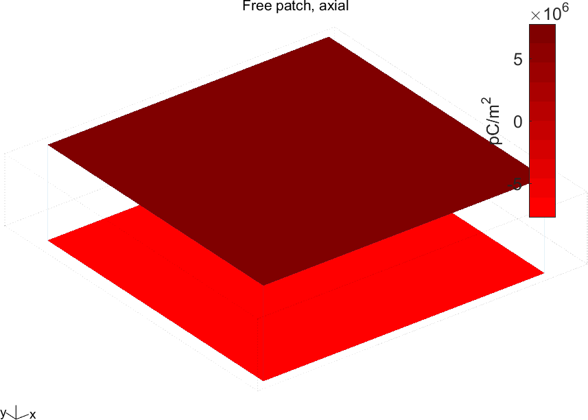
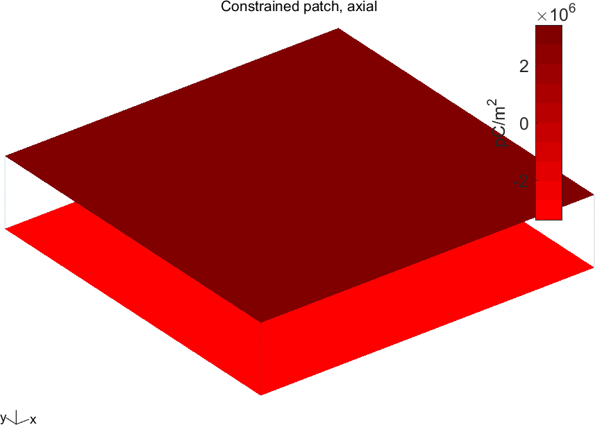
| Figure 1.7: Vizualisation of the total charge on the electrodes for the unconstrained and constrained patch under unit voltage excitation |
The results clearly show the very large difference of charge density between the two cases (free patch or constrained patch).
For this simple static example, a finer mesh can be used, but it does not lead to more accurate results (this can be done by changing the values in the call of d_piezo(′mesh′)) for example:
model=d_piezo('MeshPatch lx=1e-2 ly=1e-2 h=2e-3 nx=5 ny=5 nz=2');
model=d_piezo('MeshPatch lx=1e-2 ly=1e-2 h=2e-3 Quad');
1.2.6 Piezoelectric shear actuation
We now consider the same patch but where the polarization is in the plane of the actuator, as represented in Figure 1.8.
As in the previous example, continuous electrodes are present on the top and bottom surfaces (z=0, z=h) so that the electric potential is constant on these surfaces and denoted by V1 and V2 respectively. We assume that a difference of potential is applied between the electrodes, resulting in an electric field perpendicular to the poling direction and equal to
The electric field is now applied in direction 2, so that it will activate the shear d24=d15 mode of the piezoelectric material.

| Figure 1.8: A piezoelectric patch poled in the plane with continuous electrodes on the top and bottom surfaces |
The patch is assumed to be unconstrained so that it can expand freely, leading to {T}=0, so that we have :
We have taken into account the fact that the electric field is in the z-direction only, corresponding to direction 2 in the local axis of the piezoelectric material (direction 3 is the poling direction by convention). This shows that when the patch is poled in the plane, when applying a difference of potential across the thickness, a shear strain in the local 23 plane will be induced. The magnitude of this strain is proportional to the d24 coefficient of the piezoelectric material.
The second equation can be used in order to assess the amount of charge that is accumulated on both electrodes. We have :
The only non-zero component of the D vector is D2 given by :
The charge accumulated on the electrode is given by :
where {n} is the normal to the electrode. For the top electrode, this leads to :
where A is the surface of the electrode. For the bottom electrode
When (V1−V2) is positive, the charge on the top electrode is negative, while the charge accumulated on the bottom electrode is positive (Figure 1.5). The value of the capacitance is therefore:
which corresponds to the capacitance of the free piezoelectric patch ({T}=0) and is equal to the capacitance when the poling is out of the plane of the transducer because we have assumed є22T=є33T (in reality, there is typically a difference of 5% between these two values so that the capacitance will be slightly different).
If we now consider the case where the piezoelectric patch is fully mechanically constrained ({S}=0
), we have:
leading to :
In this case, the capacitance is given by:
which corresponds to the capacitance of the constrained piezoelectric patch ({S}=0). Note that this capacitance is clearly different from CS when the poling is out of the plane, because the value of є22S is very different from the value of є33S, due to the different values of stiffness and piezoelectric coefficients in shear and extensional mode.
1.2.7 Numerical illustration : rectangular patch in statics: shear mode
The following scripts illustrates the shear actuation using a single 8-node element as in the extension example. The patch is meshed and then the poling is aligned with the −y axis by performing a rotation of 90° around the x-axis ( d_piezo('TutoPatchShear-s1')
).
model=d_piezo('MeshPatch lx=1e-2 ly=1e-2 h=2e-3 nx=1 ny=1 nz=1');
model=p_piezo('ElectrodeMPC Top -ground',model,'z==2e-3');
model=p_piezo('ElectrodeMPC Bottom -Input "Free patch"',model,'z==0');
model.bas=basis('rotate',[],'rx=-90',1);
model=feutil('setpro 1 COORDM=1',model);
Then the response is computed both for the free case and the fully constrained case (Figure 1.9):
( d_piezo('TutoPatchShear-s2')
)
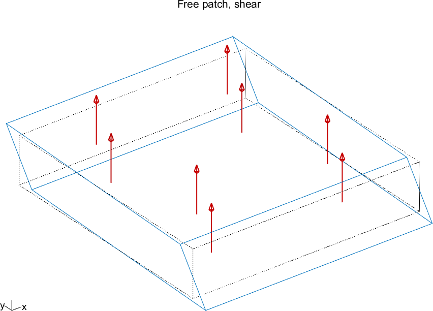
| Figure 1.9: Deformed shape of a piezoelectric patch poled in the plane with an electric field applied in the out-of-plane direction |
model=stack_set(model,'info','Freq',10);
def=fe_simul('dfrf',model); def.lab={'Free patch, shear'};
def.fun=[0 1]; def=feutil('rmfield',def,'data','LabFcn');
def=d_piezo('scriptFullConstrain',model,def);
def.lab{2}='Constrained patch, shear';
( d_piezo('TutoPatchShear-s3')
)
cf=feplot(model,def); fecom('undef line');
p_piezo('viewElec EltSel "matid1" DefLen 20e-4 reset',cf);
iimouse('zoom reset')
The mean of shear strain and stress is evaluated and compared to the d24 piezo coefficient.
Note that the mean values are computed in the global yz axis for which a negative strain corresponds to a positive strain in the local 23 axis.
Finally the capacitance is evaluated and compared to the theoretical values, showing a perfect agreement, and demonstrating the difference with the extension case for CS.
( d_piezo('TutoPatchShear-s4')
)
CC=p_piezo('viewdd -struct',cf);
a=p_piezo('viewstrain -curve -mean',cf);
fprintf('Relation between mean strain on free structure and d_24\n');
E3=a.Y(9,1); disp({'E3 mean' a.Y(9,1) 1/2e-3 'E3 analytic'})
disp([a.X{1}(4) num2cell([a.Y(4,1)/E3 CC.d(2,4)']) ...
{'d_24'}])
b=p_piezo('viewstress -curve -mean',cf);
fprintf('Relation between mean stress on pure electric and e_24 \n');
disp([b.X{1}(4) num2cell([b.Y(4,2)/-E3 CC.e(2,4)']) ...
{'e_24'}])
disp([b.X{1} num2cell(b.Y(:,2)) num2cell(a.Y(:,1)) a.X{1}])
CT=CC.epst_r(2,2)*8.854e-12*1e-2*1e-2/2e-3;
CdensT=CC.epst_r(2,2)*8.854e-12/2e-3*1e12;
CS=CC.epss_r(2,2)*8.854e-12*1e-2*1e-2/2e-3;
CdensS=CC.epss_r(2,2)*8.854e-12/2e-3*1e12;
cut=p_piezo('electrodeviewcharge',cf,struct('EltSel','matid 1'));
b=fe_caseg('stressobserve',cut,cf.def);b=reshape(b.Y,[],2);
disp([{'','CdensT','CdensS'};{'Numeric';'Theoretical'} ...
num2cell([mean(abs(b));CdensT CdensS])])
iimouse('zoom reset');
( d_piezo('TutoPatchShear-s5')
)
p_piezo('electrodeTotal',cf)
disp('Theoretical values of capacitance')
disp([{'CT';'CS'} num2cell([CT;CS])])
©1991-2019 by SDTools


 PDF Index
 PDF Index


 d_piezo('TutoPatch-s1')
. The default material is SONOX_P502_iso. The number of elements in the x, y and z directions are given by nx,ny and nz.
  d_piezo('TutoPatch-s2')
):
 d_piezo('TutoPatch-s3')
. We consider here two cases, the first one where the patch is free to expand, and the second one where it is mechanically constrained (all mechanical degrees of freedom are equal to 0).
 d_piezo('TutoPatch-s4')

 d_piezo('TutoPatch-s5')
):
 d_piezo('TutoPatch-s6')
):


 d_piezo('TutoPatchShear-s1')
).
 d_piezo('TutoPatchShear-s2')
)
 d_piezo('TutoPatchShear-s3')
)
 d_piezo('TutoPatchShear-s4')
)
 d_piezo('TutoPatchShear-s5')
)


