 PDF Index
| SDT-piezo
Contents
Functions
PDF Index |
This section explains how to mesh plates with piezoelectric patches of different shapes. In all cases, multi-layer plate elements are used to represent the host plate and the additional piezoelectric layers. The first (basic) strategy consists in assigning additional layers with given piezoelectric properties to regions of the mesh. The second approach uses a script to remesh locally the plate and add piezoelectric layers according to a predefined set of patch shapes and piezoelectric properties.
We first consider the example treated in Section 2.2, represented in Figure 2.1. The material properties of the aluminum plate and the piezoceramic patches are given in Table 2.1. The thickness of the plate is 1.2 mm, and the piezoelectric material corresponds to the SONOX_P502_iso material in m_piezo Database.

Figure 2.1: Geometric details of the aluminum plate with 4 piezoceramic patches
Property Value Aluminum plate E 72 GPa ν 0.3 ρ 2700 kg/m3 Piezoceramic patches E 54.05 GPa ν 0.41 ρ 7740 kg/m3 thickness 0.25 mm d31 -185 10−12 pC/N (or m/V) d32 -185 10−12 pC/N (or m/V) є33T 1850 є0 є0 8.854 10−12 Fm−1
Table 2.1: Material properties of the plate and the piezoceramic patches
The first step consists in meshing the plate as follows:
% See full example as MATLAB code in d_piezo('ScriptTutoPlateMeshingBasics')
%% Step 1 - Mesh the plate
 model=struct('Node',[1 0 0 0 0 0 0],'Elt',[]);
 model=feutil('addelt',model,'mass1',1);
 % Note that the extrusion values are chosen to include the patch edges
 dx=[linspace(0,15,3) linspace(15,15+55,10) linspace(15+55,463-5,50) 463];
 model=feutil('extrude 0 1 0 0',model,.001*unique(dx));
 dy=[linspace(0,12,3) linspace(12,12+25,5) linspace(12+25,63,5) ...
    linspace(63,63+25,5) linspace(63+25,100,3)];
 model=feutil('extrude 0 0 1 0',model,.001*unique(dy));
Note that the meshing is such that the patch edges corresponds to limits of elements in the mesh. It is then possible to divided the mesh in different groups, related to the two areas where the patches are added, and the host structure with no piezoelectric properties. Then a different ProID is set for the regions with piezoelectric patches.
 %% Step 2 - Set patch areas and set different properties
 model.Elt=feutil('divide group 1 withnode{x>.015 & x<.07 & y>.013 & y<.037 }',model);
 model.Elt=feutil('divide group 2 withnode{x>.015 & x<.07 & y>.064 & y<.088 }',model);
 model.Elt=feutil('set group 1 proId3',model);
 model.Elt=feutil('set group 2 proId4',model);
Visualizing the mesh and using fecom ('colordatapro') (see Figure 2.2) allows to check that different properties have been assigned to the two regions where piezoelectric patches need to be added.
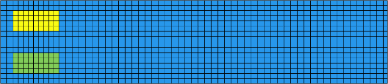
Figure 2.2: Mesh of the composite plate. The different colours represent the different groups
The next step is to define the material properties for the host structure and the patches. Here, Sonox_P502_iso is used:
%% Step 3 - Material Properties
model.pl=m_elastic('dbval 1 Aluminum');
model.pl=m_piezo(model.pl,'dbval 3 -elas2 SONOX_P502_iso');
% To avoid warning due to the use of simplified piezo properties.
model=p_piezo('DToSimple',model)
Piezoelectric material properties are divided in two parts. The first one (ProId 3 here) contains the piezoelectric data, and is linked to elastic properties with ProID 2 in this example through the -elas2 command. If the piezoelectric properties do not exist in the database, it is always possible to introduce them by hand with the following commands:
  model.pl=m_elastic('dbval 1 Aluminum');
  d=zeros(1,18); d([11 13])=560e-12; d([3 6])=-185e-12; d(9)=440e-12;
  eps=zeros(1,9); eps([1 5 9])= 8.854e-12*1850;
%                                      elasid |dij coeff  | dielectric coeffs
  model.pl=[ model.pl zeros(1,24);
            3 fe_mat('m_piezo','SI',2) 2        d           eps;
            2 fe_mat('m_elastic','SI',1) 54e9 0.41 7740 zeros(1,25)];
The piezoelectric and dielectric coefficients are stored in a vector of 18 (3x6 matrix) and 9 (3x3 matrix) values respectively. For more information see sdtweb('m_piezo').
Now that the material properties have been defined, it is necessary to create laminates with three layers, the top and bottom layers being made of the piezoelectric material (ProID 3), of thickness 0.25 mm and the middle layer being the host structure made of aluminum with thickness 1.2 mm.
%% Step 4 - Laminate properties and piezo electrodes
model.il=p_shell('dbval 1 laminate 1 1.2e-3 0', ...
  'dbval 2 laminate 3 2.5e-4 0 1 1.2e-3 0 3 2.5e-4 0');
The last step consists in assigning electrodes to each patch, and an electrical dof id. This single dof represents the difference of voltage between the top and bottom electrode and is the same for all elements in the piezoelectric patch, as the electrodes impose equipotentiality. Here for example, dof 1682.21 is assigned to the first layer of group 1, and dof 1683.21 to the third layer of the same group.
%%% Piezo electrodes
%%%                                         NdNb LayerID   NdNb  LayerID
model.il=p_piezo(model.il,'dbval 3 shell 2 1682    1   0    1683  3 0');
model.il=p_piezo(model.il,'dbval 4 shell 2 1684    1   0    1685  3 0');
We can now check that the patches are implemented properly by computing the static response to an applied voltage to the patch in group 1 (bottom). The layers are numbered from bottom to top, so it corresponds to dof 1682.21. Note that in order to find the top and bottom of an element for more complex (curved) meshes, it is possible to use the following command to show the orientation of the normal of the elements (Figure 2.3):
%% Step 5 - show orientation of the normal
feplot(model); fecom('showmap'); fecom('view3');
% scale properly
fecom('scalecoeff 1e-10'); fecom('showmap')

Figure 2.3: Mesh of the plate with arrows showing the orientation of the normals to the elements
The electrical dof corresponds to the difference of electrical potential between the top and bottom electrodes, so if one applies a difference of potential of 1V, it results in a negative electric field which is in the opposite direction of the poling direction (always in the positive z (normal) direction for a plate element). Because the d31 and d32 are negative coefficient, the resulting strain is positive (negative electric field multiplied by negative constant). A positive strain at the bottom of the plate should result in an upward motion of the tip of the beam, which is verified (Figure 2.4).
%% Step 6 - Compute and display response to static imposed voltage
model=fe_case(model,'FixDof','Cantilever','x==0 -DOF 1:6');
model=fe_case(model,'DofSet','V-Act',struct('def',1,'DOF',1682.21)); %Act
model=p_piezo('ElectrodeSensQ  1683 Q-S1',model);
model=p_piezo('ElectrodeSensQ  1684 Q-S2',model);
model=p_piezo('ElectrodeSensQ  1685 Q-S3',model);
model=fe_case(model,'SensDof','Tip',1054.03); % Displ sensor top right corner
sens=fe_case(model,'sens');
model=fe_case(model,'FixDof','SC*1683-1685',[1682:1685]+.21);
d0=fe_simul('dfrf',stack_set(model,'info','Freq',0)); % direct refer frf at 0Hz
feplot(model,d0); fecom(';view3;colordatagroup;undefline');
d=sens.cta(4,:)*d0.def % Tip displacement is positive.

Figure 2.4: Static response to a unit voltage application on one of the bottom piezoelectric patches
The script above also defines three charge sensors on dofs 1683.21, 1684.21 and 1685.21. If the electrodes are not short-circuited, it would result in a zero-charge measured, so the electrical dofs are set to zero for these three patches so that a resultant charge can be measured.
To implement a piezoelectric patch on a single side of the plate, it is important to treat properly the offset, as the layer sequence is not symmetric with respect to the neutral plane of the plate. This is done by using the z0 parameter when defining the laminates. z0 corresponds to the distance from the mid-plane to the bottom of the plate (see sdtweb ('p_shell')). The following script is the same as the previous but with piezoelectric patches only on the bottom of the plate, in which case the offset should be z0=−0.6 mm − 0.25 mm = −0.85 mm where 0.6mm is half the thickness of the support plate and 0.25mm is the thickness of the piezo.
%% Step 7 - Piezoelectric patches on the bottom only
 model=struct('Node',[1 0 0 0 0 0 0],'Elt',[]);
 model=feutil('addelt',model,'mass1',1);
 % Note that the extrusion values are chosen to include the patch edges
 dx=[linspace(0,15,3) linspace(15,15+55,10) linspace(15+55,463-5,50) 463];
 model=feutil('extrude 0 1 0 0',model,.001*unique(dx));
 dy=[linspace(0,12,3) linspace(12,12+25,5) linspace(12+25,63,5) ...
    linspace(63,63+25,5) linspace(63+25,100,3)];
 model=feutil('extrude 0 0 1 0',model,.001*unique(dy));

% Set patch areas as set different properties
 model.Elt=feutil('divide group 1 withnode{x>.015 & x<.07 & y>.013 & y<.037 }',model);
 model.Elt=feutil('divide group 2 withnode{x>.015 & x<.07 & y>.064 & y<.088 }',model);
 model.Elt=feutil('set group 1 proId3',model);
 model.Elt=feutil('set group 2 proId4',model);

%%  Material Properties
model.pl=m_elastic('dbval 1 Aluminum');
model.pl=m_piezo(model.pl,'dbval 3 -elas2 SONOX_P502_iso');
% To avoid warning due to the use of simplified piezo properties.
model=p_piezo('DToSimple',model)

%%  Laminate properties and piezo electrodes
% This is where an offset must be specified
%(else z0=-7.25e-4 (half of total thickness which is not correct).
model.il=p_shell('dbval 1 laminate 1 1.2e-3 0', ...
   'dbval 2 laminate z0=-8.5e-4 3 2.5e-4 0 1 1.2e-3 0 ');

%%% Piezo electrodes
%%%                                         NdNb LayerID
model.il=p_piezo(model.il,'dbval 3 shell 2 1682    1   0    ');
model.il=p_piezo(model.il,'dbval 4 shell 2 1684    1   0    ');

%%  Static response computation
model=fe_case(model,'FixDof','Cantilever','x==0 -DOF 1:6');
model=fe_case(model,'DofSet','V-Act',struct('def',1,'DOF',1682.21)); %Act
model=p_piezo('ElectrodeSensQ  1684 Q-S2',model);
model=fe_case(model,'SensDof','Tip',1054.03); % Displ sensor top right corner
sens=fe_case(model,'sens');
model=fe_case(model,'FixDof','SC*1682-1684',[1682 1684]+.21);
d0=fe_simul('dfrf',stack_set(model,'info','Freq',0)); % direct refer frf at 0Hz
feplot(model,d0); fecom(';view3;colordatagroup;undefline');
d=sens.cta(2,:)*d0.def % Tip displacement is positive.
when the piezoelectric element is at the top of the plate, then the offset should be equal to the thickness of the main plate divided by two (negative value).
The automated procedure requires the plate model to be defined in mm. In order to add the patches, one needs to make a structure which contains the initial plate model and a description of the different patches to be added. In this example, the patches are assigned with +Rect.Sonox_P502_iso.5525TH0_25 where the sign +/- specifies if the patch is on the top (+) or the bottom (-) of the plate, the first argument gives the geometry (Rect for Rectangular), the second argument is the piezoelectric material type from the database, the next argument is the size (55mm x 25mm here) and the last argument is the thickness (0.25mm). So the first step is to make the host plate. Here, we define a mesh so that the edges of the piezoelectric patches will correspond to the mesh (as in the previous example of meshing manually).
% See full example as MATLAB code in d_piezo('ScriptTutoPlateMeshingAuto')
%% Step 1 : model of host plate -
 model=struct('Node',[1 0 0 0 0 0 0],'Elt',[]);
 model=feutil('addelt',model,'mass1',1);
 % Note that the extrusion values are chosen to include the patch edges
 dx=[linspace(0,15,3) linspace(15,15+55,10) linspace(15+55,463-5,50) 463];
 model=feutil('extrude 0 1 0 0',model,unique(dx));
 dy=[linspace(0,12,3) linspace(12,12+25,5) linspace(12+25,63,5) ...
    linspace(63,63+25,5) linspace(63+25,100,3)];
 model=feutil('extrude 0 0 1 0',model,unique(dy));
model.unit='mm';

% Material Properties
model.pl=m_elastic('dbval 1 Aluminum');
% Laminate properties
model.il=p_shell('dbval 1 -punit mm laminate 1 1.2 0') % this is to specify in mm
model=fe_case(model,'FixDof','Cantilever','x==0 -DOF 1:6');
The model should is defined in mm to use the automated procedure. Then we will add four rectangular piezoelectric patches whose size and shape comply with the mesh.
%% Step 2: Add patches
RG.list={'Name','Lam','shape'
   'Main_plate', model,''  % Base structure
   'Act1', ... % name of patch
   'BaseId1 +Rect.Sonox_P502_iso.5525TH0_25 -Rect.Sonox_P502_iso.5525TH0_25', ...
     struct('shape','LsRect', ... % Remeshing strategy (lsutil rect here)
       'xc',15+55/2,'yc',12+25/2,'alpha',0,'tolE',.1)
    'Act2', ... % name of patch
   'BaseId1 +Rect.Sonox_P502_iso.5525TH0_25 -Rect.Sonox_P502_iso.5525TH0_25', ...
     struct('shape','LsRect', ... % Remeshing strategy (lsutil rect here)
       'xc',15+55/2,'yc',63+25/2,'alpha',0,'tolE',.1)
       };
mo1=d_piezo('MeshPlate',RG);
mo1=stack_rm(mo1,'info','Electrodes'); % Obsolete stack field to be removed
% To avoid warning due to the use of simplified piezo properties.
mo1=p_piezo('DToSimple',mo1)
The command +Rect.Sonox_P502_iso.5525TH0_25 refers to a patch which is added on the top of the plate (+), is rectangular (Rect), is made of Sonox_P502_iso, is of size 55mmx25mm (5525) and thickness 0.25mm (TH0_25). Then we need to specify the position of the patch with 'xc' and 'yc' which correspond to the coordinates of its center. The model obtained is here the same as the one previously obtained with manual meshing. The static response when actuating the first piezo patch is then computed:
%% Step 3 : compute response
nd=feutil('find node x==463 & y==100',model);
elnd=floor(p_piezo('electrodedof.*',mo1)); % Nodes associated to electrodes
mo1=fe_case(mo1,'SensDof','Tip',nd+.03); % Displ sensor
mo1=fe_case(mo1,'DofSet','V-Act',struct('def',1,'DOF',elnd(1)+.21)); %Act
mo1=p_piezo(['ElectrodeSensQ  ' num2str(elnd(1)) ' Q-Act'],mo1); % Charge sensors
mo1=p_piezo(['ElectrodeSensQ ' num2str(elnd(2)) ' Q-S1'],mo1);
mo1=p_piezo(['ElectrodeSensQ ' num2str(elnd(3)) ' Q-S2'],mo1);
mo1=p_piezo(['ElectrodeSensQ ' num2str(elnd(4)) ' Q-S3'],mo1);

% Fix last 3 elec dofs to measure resultant (charge)
mo1=fe_case(mo1,'FixDof', ...
['SC*' num2str(elnd(2)) '/' num2str(elnd(3)) '/' num2str(elnd(4)) ], ...
elnd([2:4])+.21);
sens=fe_case(mo1,'sens');

d1=fe_simul('dfrf',stack_set(mo1,'info','Freq',0)); % direct refer frf at 0Hz
d1t=sens.cta(1,:)*d1.def; % Extract tip displ
feplot(mo1,d1);
fecom('colordatapro'); fecom('view3');
Note that the automated meshing introduces the patches in the order of the description, so that here the first piezoelectric patch is on the top (+), and the static response is downwards. Automated meshing can also be done when the patch edges do not coincide with the mesh of the host plate. In this case, automated local remeshing is applied. We take the example of an initial mesh of the plate with a uniform mesh of prescribed element size (here around 7 mm). The script to add the four patches is strictly identical, but the result is different due to the local remeshing.
%% Step 4 : use local remeshing element size is 7 mm
 model=feutil('objectquad 1 1',[0 0 0;1 0 0;0 1 0], ...
    feutil('refineline 7',[0 463]), ...
    feutil('refineline 7',[0 100]));
     model.unit='mm';
% Material Properties
model.pl=m_elastic('dbval 1 Aluminum');
% Laminate properties
model.il=p_shell('dbval 1 -punit mm laminate 1 1.2 0') % this is to specify in mm
model=fe_case(model,'FixDof','Cantilever','x==0 -DOF 1:6');

%% Add patches
RG.list={'Name','Lam','shape'
   'Main_plate', model,''  % Base structure
   'Act1', ... % name of patch
   'BaseId1 +Rect.Sonox_P502_iso.5525TH0_25 -Rect.Sonox_P502_iso.5525TH0_25', ...
     struct('shape','LsRect', ... % Remeshing strategy (lsutil rect here)
       'xc',15+55/2,'yc',12+25/2,'alpha',0,'tolE',.1)
    'Act2', ... % name of patch
   'BaseId1 +Rect.Sonox_P502_iso.5525TH0_25 -Rect.Sonox_P502_iso.5525TH0_25', ...
     struct('shape','LsRect', ... % Remeshing strategy (lsutil rect here)
       'xc',15+55/2,'yc',63+25/2,'alpha',0,'tolE',.1)
       };
mo2=d_piezo('MeshPlate',RG);
mo2=stack_rm(mo2,'info','Electrodes'); % Obsolete stack field to be removed
% To avoid warning due to the use of simplified piezo properties.
mo2=p_piezo('DToSimple',mo2)

nd=feutil('find node x==463 & y==100',model);
elnd=floor(p_piezo('electrodedof.*',mo2)); % Nodes associated to electrodes
mo2=fe_case(mo2,'SensDof','Tip',nd+.03); % Displ sensor
mo2=fe_case(mo2,'DofSet','V-Act',struct('def',1,'DOF',elnd(1)+.21)); %Act
mo2=p_piezo(['ElectrodeSensQ  ' num2str(elnd(1)) ' Q-Act'],mo2); % Charge sensors
mo2=p_piezo(['ElectrodeSensQ ' num2str(elnd(2)) ' Q-S1'],mo2);
mo2=p_piezo(['ElectrodeSensQ ' num2str(elnd(3)) ' Q-S2'],mo2);
mo2=p_piezo(['ElectrodeSensQ ' num2str(elnd(4)) ' Q-S3'],mo2);

% Fix last 3 elec dofs to measure resultant (charge)
mo2=fe_case(mo2,'FixDof', ...
['SC*' num2str(elnd(2)) '/' num2str(elnd(3)) '/' num2str(elnd(4)) ], ...
elnd([2:4])+.21);
sens=fe_case(mo2,'sens');

d2=fe_simul('dfrf',stack_set(mo2,'info','Freq',0)); % direct refer frf at 0Hz
d2t=sens.cta(1,:)*d2.def;

feplot(mo2,d2);
fecom('colordatapro'); fecom('view3');
[d1t d2t]
The values of d1t and d2t correspond to the tip displacement when actuating the first piezo patch, for the first model where the edges of the piezos correspond to the element sides in the mesh, and when there is a local remeshing. Due to the effect of the local remeshing (Figure 2.5), there is a slight difference (2%). In order to check this effect, we can use a finer mesh of the host structure and check for the convergence.

Figure 2.5: Static response to a unit voltage application on one of the bottom piezoelectric patches
%% Step 5 : use a finer mesh to check convergence
ref=[5 3 2];
dt=[d2t];

for ij=1:length(ref)

 model=feutil('objectquad 1 1',[0 0 0;1 0 0;0 1 0], ...
    feutil(['refineline ' num2str(ref(ij))],[0 463]), ...
    feutil(['refineline ' num2str(ref(ij))],[0 100]));
     model.unit='mm';
% Material Properties
model.pl=m_elastic('dbval 1 Aluminum');
% Laminate properties
model.il=p_shell('dbval 1 -punit mm laminate 1 1.2 0') % this is to specify in mm
model=fe_case(model,'FixDof','Cantilever','x==0 -DOF 1:6');

%% Add patches
RG.list={'Name','Lam','shape'
   'Main_plate', model,''  % Base structure
   'Act1', ... % name of patch
   'BaseId1 +Rect.Sonox_P502_iso.5525TH0_25 -Rect.Sonox_P502_iso.5525TH0_25', ...
     struct('shape','LsRect', ... % Remeshing strategy (lsutil rect here)
       'xc',15+55/2,'yc',12+25/2,'alpha',0,'tolE',.1)
    'Act2', ... % name of patch
   'BaseId1 +Rect.Sonox_P502_iso.5525TH0_25 -Rect.Sonox_P502_iso.5525TH0_25', ...
     struct('shape','LsRect', ... % Remeshing strategy (lsutil rect here)
       'xc',15+55/2,'yc',63+25/2,'alpha',0,'tolE',.1)
       };
mo2=d_piezo('MeshPlate',RG);
mo2=stack_rm(mo2,'info','Electrodes'); % Obsolete stack field to be removed
% To avoid warning due to the use of simplified piezo properties.
mo2=p_piezo('DToSimple',mo2)

nd=feutil('find node x==463 & y==100',model);
elnd=floor(p_piezo('electrodedof.*',mo2)); % Nodes associated to electrodes
mo2=fe_case(mo2,'SensDof','Tip',nd+.03); % Displ sensor
mo2=fe_case(mo2,'DofSet','V-Act',struct('def',1,'DOF',elnd(1)+.21)); %Act
mo2=p_piezo(['ElectrodeSensQ  ' num2str(elnd(1)) ' Q-Act'],mo2); % Charge sensors
mo2=p_piezo(['ElectrodeSensQ ' num2str(elnd(2)) ' Q-S1'],mo2);
mo2=p_piezo(['ElectrodeSensQ ' num2str(elnd(3)) ' Q-S2'],mo2);
mo2=p_piezo(['ElectrodeSensQ ' num2str(elnd(4)) ' Q-S3'],mo2);

% Fix last 3 elec dofs to measure resultant (charge)
mo2=fe_case(mo2,'FixDof', ...
['SC*' num2str(elnd(2)) '/' num2str(elnd(3)) '/' num2str(elnd(4)) ], ...
elnd([2:4])+.21);
sens=fe_case(mo2,'sens');

d2=fe_simul('dfrf',stack_set(mo2,'info','Freq',0)); % direct refer frf at 0Hz
d2t=sens.cta(1,:)*d2.def;

dt=[dt; d2t];
end

figure; plot([7 ref],1e6*dt,'linewidth',2); set(gca, 'XDir','reverse');
set(gca,'Fontsize',15); v=get(gca,'XLim'); hold on;
plot(v,1e6*[d1t d1t],'r','linewidth',2);
xlabel('mesh size (mm)'); ylabel('tip displacement (mm/V)')

Figure 2.6: Convergence of the tip displacement when the size of the elements of the main plate is varied. The red line corresponds to the tip displacement with the mesh conforming with the patch edges
We see that when the plate mesh is finer (Figure 2.6), the local effect of remeshing is less and we converge to the tip displacement when the piezoelectric patch edges coincide with the mesh. A last example is the addition of circular patches, where we also check for convergence:
%% Step 6 : with circular patches
  model=feutil('objectquad 1 1',[0 0 0;1 0 0;0 1 0], ...
    feutil('refineline 7',[0 463]), ...
    feutil('refineline 7',[0 100]));
     model.unit='mm';

%%%%%% Material Properties
model.pl=m_elastic('dbval 1 Aluminum');
%%%%% Laminate properties
model.il=p_shell('dbval 1 -punit mm laminate 1 1.2 0') % this is to specify in mm

model=fe_case(model,'FixDof','Cantilever','x==0 -DOF 1:6');

RG.list={'Name','Lam','shape'
   'Main_plate', model,''  % Base structure
   'Act1', ... % name of patch
   'BaseId1 +Disk.Sonox_P502_iso.RC10TH1 -Disk.Sonox_P502_iso.RC10TH1', ...
   struct('shape','lscirc','xc',15+55/2,'yc',12+25/2),
   'Act2', ... % name of patch
   'BaseId1 +Disk.Sonox_P502_iso.RC10TH1 -Disk.Sonox_P502_iso.RC10TH1', ...
   struct('shape','lscirc','xc',15+55/2,'yc',63+25/2)};

%
mo3=d_piezo('MeshPlate',RG);
mo3=stack_rm(mo3,'info','Electrodes'); % Old Stack not necessary or should be set to 0
mo3.pl([3 5 7 9],7)=0; % Set damping to zero in Noliac otherwise complex static response
% To avoid warning due to the use of simplified piezo properties.
mo3=p_piezo('DToSimple',mo3)

nd=feutil('find node x==463 & y==100',model);
elnd=floor(p_piezo('electrodedof.*',mo3)); % Nodes associated to electrodes
mo3=fe_case(mo3,'SensDof','Tip',nd+.03); % Displ sensor
mo3=fe_case(mo3,'DofSet','V-Act',struct('def',1,'DOF',elnd(1)+.21)); %Act
mo3=p_piezo(['ElectrodeSensQ  ' num2str(elnd(1)) ' Q-Act'],mo3); % Charge sensors
mo3=p_piezo(['ElectrodeSensQ ' num2str(elnd(2)) ' Q-S1'],mo3);
mo3=p_piezo(['ElectrodeSensQ ' num2str(elnd(3)) ' Q-S2'],mo3);
mo3=p_piezo(['ElectrodeSensQ ' num2str(elnd(4)) ' Q-S3'],mo3);

% Fix last 3 elec dofs to measure resultant (charge)
mo3=fe_case(mo3,'FixDof', ...
['SC*' num2str(elnd(2)) '/' num2str(elnd(3)) '/' num2str(elnd(4)) ], ...
elnd([2:4])+.21);
sens=fe_case(mo3,'sens');

d3=fe_simul('dfrf',stack_set(mo3,'info','Freq',0)); % direct refer frf at 0Hz
d3t=sens.cta(1,:)*d3.def; % First electrode is on top now ?

feplot(mo3,d3)
fecom('colordatapro'); fecom('view3');

[d1t d2t d3t]
The local remeshing can be see in Figure 2.7. Note that here, we use a predefined patch type. The predefined types are obtained with m_piezo ('patch'). And their used is further explained in the next section.

Figure 2.7: Static response to a unit voltage application on one of the bottom circular piezoelectric patches
%% Step 7 : Check convergence

ref=[5 3 2];
dt=[d3t];

for ij=1:length(ref)

 model=feutil('objectquad 1 1',[0 0 0;1 0 0;0 1 0], ...
    feutil(['refineline ' num2str(ref(ij))],[0 463]), ...
    feutil(['refineline ' num2str(ref(ij))],[0 100]));
     model.unit='mm';
% Material Properties
model.pl=m_elastic('dbval 1 Aluminum');
% Laminate properties
model.il=p_shell('dbval 1 -punit mm laminate 1 1.2 0') % this is to specify in mm
model=fe_case(model,'FixDof','Cantilever','x==0 -DOF 1:6');

RG.list={'Name','Lam','shape'
   'Main_plate', model,''  % Base structure
   'Act1', ... % name of patch
   'BaseId1 +Disk.Sonox_P502_iso.RC10TH1 -Disk.Sonox_P502_iso.RC10TH1', ...
   struct('shape','lscirc','xc',15+55/2,'yc',12+25/2),
   'Act2', ... % name of patch
   'BaseId1 +Disk.Sonox_P502_iso.RC10TH1 -Disk.Sonox_P502_iso.RC10TH1', ...
   struct('shape','lscirc','xc',15+55/2,'yc',63+25/2)};

%
mo3=d_piezo('MeshPlate',RG);
mo3=stack_rm(mo3,'info','Electrodes'); % Old Stack not necessary or should be set to 0
mo3.pl([3 5 7 9],7)=0; % Set damping to zero in Noliac otherwise complex static response
% To avoid warning due to the use of simplified piezo properties.
mo3=p_piezo('DToSimple',mo3)

nd=feutil('find node x==463 & y==100',model);
elnd=floor(p_piezo('electrodedof.*',mo3)); % Nodes associated to electrodes
mo3=fe_case(mo3,'SensDof','Tip',nd+.03); % Displ sensor
mo3=fe_case(mo3,'DofSet','V-Act',struct('def',1,'DOF',elnd(1)+.21)); %Act
mo3=p_piezo(['ElectrodeSensQ  ' num2str(elnd(1)) ' Q-Act'],mo3); % Charge sensors
mo3=p_piezo(['ElectrodeSensQ ' num2str(elnd(2)) ' Q-S1'],mo3);
mo3=p_piezo(['ElectrodeSensQ ' num2str(elnd(3)) ' Q-S2'],mo3);
mo3=p_piezo(['ElectrodeSensQ ' num2str(elnd(4)) ' Q-S3'],mo3);

% Fix last 3 elec dofs to measure resultant (charge)
mo3=fe_case(mo3,'FixDof', ...
['SC*' num2str(elnd(2)) '/' num2str(elnd(3)) '/' num2str(elnd(4)) ], ...
elnd([2:4])+.21);
sens=fe_case(mo3,'sens');

d3=fe_simul('dfrf',stack_set(mo3,'info','Freq',0)); % direct refer frf at 0Hz
d3t=sens.cta(1,:)*d3.def; % First electrode is on top now ?

dt=[dt; d3t];
end

figure; plot([7 ref],1e6*(dt),'linewidth',2); set(gca, 'XDir','reverse');
set(gca,'Fontsize',15)
xlabel('mesh size (mm)'); ylabel('tip displacement (mm/V)')
The convergence of the tip displacement can be see in Figure 2.8.

Figure 2.8: Convergence of the tip displacement when the size of the elements of the main plate is varied, for a circular piezoelectric patch
The different types of patches that can be integrated in plate meshes can be seen by typing the command m_piezo 'patch'. At the moment of writing this documentation, the output is
    {'Noliac.NCE51.RC12TH1'  }    {'Noliac, material, disk ODiameter and THickness'}
    {'SmartM.MFC-P1.2814'    }    {'Smart materials MFC d33, .WiLe (dims mm)'     }
    {'SmartM.MFC-P2.2814'    }    {'Smart materials MFC d31, .WiLe (dims mm)'     }
    {'Disk.Material.RC12TH1' }    {'Circular patch, material, geometry'           }
    {'Rect.Material.2814TH_5'}    {'Rectangular patch, material, geometry'        }
The last two types of patches are the ones used in the previous scripts, which correspond to rectangular and circular patches, for which the material can be chosen, as well as the geometrical properties. There also exist on the market packaged piezoelectric patches which are made of several layers, such as the Macro Fiber Composite (https://smart-material.com). The properties of the different layers are described in more details in 2.3. Two types of MFCs exist (P1, and P2). The Noliac patch is a disk, and could be described with the generic Disk.Material.RCXXTHX command.
The following example is the integration of two P1-type MFC patches on a beam. The example is further discussed in Section 2.3.2, the resulting mesh is represented in Figure ??.
% See full example as MATLAB code in d_piezo('ScriptTutoPlateMeshingMFC')
% Create mesh. Geometric properties in the manual
RO=struct('L',463,'w',50,'a',85,'b',28,'c',15,'d',11);

% create a rectangle with targetl = 3 mm
 model=feutil('objectquad 1 1',[0 0 0;1 0 0;0 1 0], ...
    feutil('refineline 5',[0 RO.c+[0 RO.a] RO.L]), ...
    feutil('refineline 5',[0 RO.d+[0 RO.b] RO.w]));
%%%%% Material Properties for supporting plate
 model.pl=m_elastic('dbval 1 -unit MM Aluminum'); % Aluminum
 model.il=p_shell('dbval 1 -punit MM laminate 1 1 0');
 model.unit='MM';

RG.list={'Name','Lam','shape'
   'Main_plate', model,''  % Base structure
   'Act1', ... % name of patch
   'BaseId1 +SmartM.MFC-P1.8528 -SmartM.MFC-P1.8528', ... % Layout definition
     struct('shape','LsRect', ... % Remeshing strategy (lsutil rect here)
       'xc',RO.c+RO.a/2,'yc',RO.d+RO.b/2,'alpha',0,'tolE',.1)
       };

mo1=d_piezo('MeshPlate',RG);
feplot(mo1); fecom(';colordatapro;view3');

Figure 2.9: Mesh of the plate with MFC transducers on top and bottom. The different colours represent the different groups

